- 您现在的位置:买卖IC网 > Sheet目录336 > IXDN514SIAT/R (IXYS)IC GATE DRIVER SGL 14A 8-SOIC
�� �
�
�IXDI514� /� IXDN514�
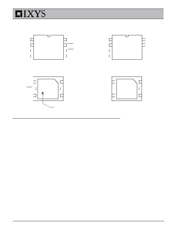
�PIN� CONFIGURATIONS�
�8� PIN� DIP� (PI)�
�8� PIN� SOIC� (SIA)�
�8� PIN� DIP� (PI)�
�8� PIN� SOIC� (SIA)�
�VCC�
�1�
�I�
�8�
�VCC�
�VCC�
�1�
�I�
�8�
�VCC�
�X�
�X�
�IN�
�2�
�D�
�7�
�OUT�
�IN�
�2�
�D�
�7�
�OUT�
�I�
�N�
�NC�
�GND�
�3�
�4�
�5�
�1�
�4�
�6�
�5�
�OUT�
�GND�
�NC�
�GND�
�3�
�4�
�5�
�1�
�4�
�6�
�5�
�OUT�
�GND�
�6� LEAD� DFN� (D1)�
�(Bottom� View)�
�6� LEAD� DFN� (D1)�
�(Bottom� View)�
�VCC� 6�
�I�
�X�
�1� IN�
�VCC� 6�
�I�
�X�
�1� IN�
�D�
�D�
�OUT� 5�
�I�
�2� N/C�
�OUT� 5�
�N�
�2� N/C�
�5�
�5�
�GND�
�4�
�1�
�4�
�3� GND�
�GND�
�4�
�1�
�4�
�3� GND�
�NOTE:� Solder� tabs� on� bottoms� of� DFN� packages� are� grounded�
�Supply Bypassing, Grounding Practices And Output Lead inductance�
�When� designing� a� circuit� to� drive� a� high� speed� MOSFET�
�utilizing� the� IXD_514,� it� is� very� important� to� observe� certain�
�design� criteria� in� order� to� optimize� performance� of� the� driver.�
�Particular� attention� needs� to� be� paid� to� Supply� Bypassing� ,�
�Grounding� ,� and� minimizing� the� Output� Lead� Inductance� .�
�Say,� for� example,� we� are� using� the� IXD_514� to� charge� a� 5000pF�
�capacitive� load� from� 0� to� 25� volts� in� 25ns� .�
�Using� the� formula:� I=� ?� V� C� /� ?� t,� where� ?� V=25V� C=5000pF� &�
�?� t=25ns,� we� can� determine� that� to� charge� 5000pF� to� 25� volts�
�in� 25ns� will� take� a� constant� current� of� 5A.� (In� reality,� the� charging�
�current� won’t� be� constant,� and� will� peak� somewhere� around�
�8A).�
�SUPPLY� BYPASSING�
�In� order� for� our� design� to� turn� the� load� on� properly,� the� IXD_514�
�must� be� able� to� draw� this� 5A� of� current� from� the� power� supply�
�in� the� 25ns.� This� means� that� there� must� be� very� low� impedance�
�between� the� driver� and� the� power� supply.� The� most� common�
�method� of� achieving� this� low� impedance� is� to� bypass� the� power�
�supply� at� the� driver� with� a� capacitance� value� that� is� an� order� of�
�magnitude� larger� than� the� load� capacitance.� Usually,� this�
�would� be� achieved� by� placing� two� different� types� of� bypassing�
�capacitors,� with� complementary� impedance� curves,� very� close�
�to� the� driver� itself.� (These� capacitors� should� be� carefully�
�selected� and� should� have� low� inductance,� low� resistance� and�
�high-pulse� current-service� ratings).� Lead� lengths� may� radiate�
�at� high� frequency� due� to� inductance,� so� care� should� be� taken�
�to� keep� the� lengths� of� the� leads� between� these� bypass�
�capacitors� and� the� IXD_514� to� an� absolute� minimum.�
�11�
�GROUNDING�
�In� order� for� the� design� to� turn� the� load� off� properly,� the� IXD_514�
�must� be� able� to� drain� this� 5A� of� current� into� an� adequate�
�grounding� system.� There� are� three� paths� for� returning� current�
�that� need� to� be� considered:� Path� #1� is� between� the� IXD_514�
�and� its� load.� Path� #2� is� between� the� IXD_514� and� its� power�
�supply.� Path� #3� is� between� the� IXD_514� and� whatever� logic� is�
�driving� it.� All� three� of� these� paths� should� be� as� low� in� resistance�
�and� inductance� as� possible,� and� thus� as� short� as� practical.� In�
�addition,� every� effort� should� be� made� to� keep� these� three�
�ground� paths� distinctly� separate.� Otherwise,� the� returning�
�ground� current� from� the� load� may� develop� a� voltage� that� would�
�have� a� detrimental� effect� on� the� logic� line� driving� the� IXD_514.�
�OUTPUT� LEAD� INDUCTANCE�
�Of� equal� importance� to� Supply� Bypassing� and� Grounding� are�
�issues� related� to� the� Output� Lead� Inductance.� Every� effort�
�should� be� made� to� keep� the� leads� between� the� driver� and� its�
�load� as� short� and� wide� as� possible.� If� the� driver� must� be� placed�
�farther� than� 2”� (5mm)� from� the� load,� then� the� output� leads�
�should� be� treated� as� transmission� lines.� In� this� case,� a� twisted-�
�pair� should� be� considered,� and� the� return� line� of� each� twisted�
�pair� should� be� placed� as� close� as� possible� to� the� ground� pin�
�of� the� driver,� and� connected� directly� to� the� ground� terminal� of� the�
�load.�
�发布紧急采购,3分钟左右您将得到回复。
相关PDF资料
IXDN602PI
MOSFET N-CH 2A DUAL LO SIDE 8-DI
IXDN630CI
IC GATE DRIVER LOW SIDE 5TO220
IXDS430SI
IC DRVR MOSF/IGBT 30A 28-SOIC
IXS839S1T/R
IC MOSFET DRIVER SYNC BUCK 8SOIC
JLINK-RX-AD
ADAPT BD FOR MINI-JTAG CONNECTOR
JMBADGE2008-B
BOARD JM BADGE
JP9902
CONN JACK MOD INSERT W/O HOLES
JTAGJET-C2000
JTAG EMULATOR FOR TI C2000 MCU
相关代理商/技术参数
IXDN514SIATR
制造商:IXYS 制造商全称:IXYS Corporation 功能描述:14 Ampere Low-Side Ultrafast MOSFET Drivers
IXDN55N120
制造商:IXYS 制造商全称:IXYS Corporation 功能描述:High Voltage IGBT with optional Diode
IXDN55N120AU1
制造商:未知厂家 制造商全称:未知厂家 功能描述:TRANSISTOR | IGBT | N-CHAN | 1.2KV V(BR)CES | 85A I(C) | SOT-227B
IXDN55N120D1
功能描述:IGBT 晶体管 55 Amps 1200V RoHS:否 制造商:Fairchild Semiconductor 配置: 集电极—发射极最大电压 VCEO:650 V 集电极—射极饱和电压:2.3 V 栅极/发射极最大电压:20 V 在25 C的连续集电极电流:150 A 栅极—射极漏泄电流:400 nA 功率耗散:187 W 最大工作温度: 封装 / 箱体:TO-247 封装:Tube
IXDN602D2TR
功能描述:IC GATE DVR 2A DUAL HS 8DFN RoHS:是 类别:集成电路 (IC) >> PMIC - MOSFET,电桥驱动器 - 外部开关 系列:- 标准包装:50 系列:- 配置:低端 输入类型:非反相 延迟时间:40ns 电流 - 峰:9A 配置数:1 输出数:1 高端电压 - 最大(自引导启动):- 电源电压:4.5 V ~ 35 V 工作温度:-40°C ~ 125°C 安装类型:表面贴装 封装/外壳:TO-263-6,D²Pak(5 引线+接片),TO-263BA 供应商设备封装:TO-263 包装:管件
IXDN602PI
功能描述:MOSFET N-CH 2A DUAL LO SIDE 8-DI RoHS:是 类别:集成电路 (IC) >> PMIC - MOSFET,电桥驱动器 - 外部开关 系列:- 标准包装:95 系列:- 配置:高端和低端,独立 输入类型:非反相 延迟时间:160ns 电流 - 峰:290mA 配置数:1 输出数:2 高端电压 - 最大(自引导启动):600V 电源电压:10 V ~ 20 V 工作温度:-40°C ~ 125°C 安装类型:表面贴装 封装/外壳:8-SOIC(0.154",3.90mm 宽) 供应商设备封装:8-SOIC 包装:管件 产品目录页面:1381 (CN2011-ZH PDF)
IXDN602SI
功能描述:MOSFET N-CH 2A DUAL LO SIDE 8-SO RoHS:是 类别:集成电路 (IC) >> PMIC - MOSFET,电桥驱动器 - 外部开关 系列:- 标准包装:95 系列:- 配置:半桥 输入类型:PWM 延迟时间:25ns 电流 - 峰:1.6A 配置数:1 输出数:2 高端电压 - 最大(自引导启动):118V 电源电压:9 V ~ 14 V 工作温度:-40°C ~ 125°C 安装类型:表面贴装 封装/外壳:8-SOIC(0.154",3.90mm 宽) 供应商设备封装:8-SOIC 包装:管件 产品目录页面:1282 (CN2011-ZH PDF) 其它名称:*LM5104M*LM5104M/NOPBLM5104M
IXDN602SIA
功能描述:DUAL LOW SIDE MOSFET DRIVER RoHS:是 类别:集成电路 (IC) >> PMIC - MOSFET,电桥驱动器 - 外部开关 系列:- 标准包装:95 系列:- 配置:高端和低端,独立 输入类型:非反相 延迟时间:160ns 电流 - 峰:290mA 配置数:1 输出数:2 高端电压 - 最大(自引导启动):600V 电源电压:10 V ~ 20 V 工作温度:-40°C ~ 125°C 安装类型:表面贴装 封装/外壳:8-SOIC(0.154",3.90mm 宽) 供应商设备封装:8-SOIC 包装:管件 产品目录页面:1381 (CN2011-ZH PDF)